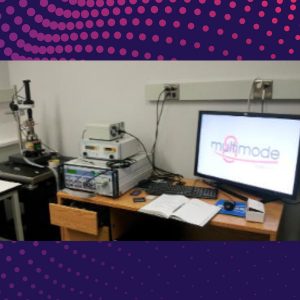
Scanning electron microscope – focused ion beam (SEM-FIB)
Scanning electron microscope – focused ion beam (SEM-FIB)
Additional information
| MANUFACTURER | Tescan |
|---|---|
| MODEL | Lyra3 |
Description
- Focused Ion Beam (FIB) integrated with a Scanning electronic microscopy (SEM) for TEM sample preparation
- Gas Injection System (GIS) to deposit and etch (5-GIS de Orsayphysics) equipped with 5 precursors
- Nanomanipulateur OmniProbe 200 d’Oxford Instrument
- Characterization by energy dispersive spectroscopy (EDS) (Quantax from Bruker, X-Flash 6160 detector)
Applications
- Nanometric scale sample observation (SEM) via secondary (SE) or backscattered (BSE) electron emission
- X-ray elemental analysis (EDS)
- Nanometric scale etching (FIB)
- Multilayer coatings cross section analysis (FIB-SEM)
Technical specifications
- Electron optics
- Electron gun: – High-brightness Schottky source, acceleration voltage 0.2-30kV
- Probe current : 2pA – 200nA
- Resolution: SE mode, 1.2 nm at 30 kV and 3.0 nm at 3 kV. BSE mode, 2.0 nm at 30kV
- Magnification : 1X – 1,000,000X
- Ion gun : liquid Galium
- Resolution : < 5 nm at 30 kV / < 2.5 nm at 30 kV (at the MEB-FIB coincidence point)
- Magnification : 150X – 1,000,000X
- SEM-FIB angle : 55o
- Acceleration voltage : 0.5kV – 30 kV
To use this equipment
The equipment available is accessible to the academic and industrial research community.
To learn about the terms of use and availability, please complete the form below. After reviewing your request, we will get in touch with you promptly to offer the best available solution.
